Why?
The FBUS master feature requires to do some IO multiplexing so I would have needed to build ardware anyways. That’s why I’ve decided to put the learnings of the past months into a single design. And of course this will allow a more convenient devleopment experience.
- Drivers development for new sensors
- SPI and I2C broken out to solder pads
- All UARTS accessible for testing
- individually configurable servo ouptus: FBUS/PWM
- putting as much hardware as possible into one plattform
- easily accesible SWD connector
- SWD on USB-C
Features
But what else does it offer?
What are its components and features?
While adding some new stuff I tried to include all the latest features and what a maxed out flight controller could possibly offer. Because in the end this thing will be sitting on a desk and be used for testing new sw-features and hardware.
Maybe it could also be used for continous integration?
But what are the exact lessons learned which went into this design? Some of that stuff is quite obvisous but due to having very small PCBs I could (or simply did not?) take care of these aspects.
- separating the GNDs of different supply nets to allow current flow on defined paths only
- moving the buck converter away from the MCU’s oscillator
- distributing power poroperly across the different components
- STM32F722
- 2 sizes of flash memory connectable
- Baro: BMP581 and DPS368
- IMU: BMI088 and BMI270/321
- Power supply for servos
- RX connectors: DSMX/ELRS/FBUS
- Servo connectors: S1-S4, M1,M2
- WS2812 LED
- 2 system LEDs
- Split power supply: MCU/RX/sensors
- SPI1 and I2C1, open GPIOs broken out
- test pads for the supply voltages
- ADC for battery and BEC
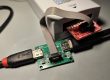
SWD on USB-C
What the hell is SWD on USB-C? In m past few projects I’ve used a schematic like this one. The SBU pins of the USB-C header are mostly left unused. These are the sideband use pins for the alternate modes. Unless a device implements this and requests the alternate mode, nothing is going on on these pins.
I’ve desiugned breakout boards and adapters to inject SWD signals from a J-Link into the USB-C cable. So I can easily do in-system debugging and programming, as long as the USB-C connector is accessible.
But this comes with two slight downsides:
- you need to use a fully connected USB-C cable between the target and the breakout board. Charger cables or USB 2.0 cables won’t work.
- You need to connect the cable in the „right“ orientation. Flipping the connector won’t cause any damage but the debugging just won’t work. USB-C doubles each pin to be able to connect the cable either way. SBU1/2 are actually such a pair, but since I am having a different signal on each pin, I kind of break the symmetry.
This does not comply to USB spec, but it is convenient to use and just works!
Where did I get the idea from? Mainly from these two sources:

Next Steps
Order has been placed at JLCPCB, the BOM has been created at Mouser electronics. And another lessen: ordered the solder stencil aswell. Dispensing the paste manually is just worth the hassle and the results aren’t that great.
So once the PCB arrives I can start assembling it. To be continued ….